|
iSensor-SPI-Buffer
1.15
Firmware for the iSensor-SPI-Buffer board to enable full throughput buffered data capture on Analog Devices IMUs
|
|
iSensor-SPI-Buffer
1.15
Firmware for the iSensor-SPI-Buffer board to enable full throughput buffered data capture on Analog Devices IMUs
|
Data and control interfacing to the iSensor SPI Buffer firmware from a master device is done via a set of 16-bit user accessible registers. These registers can be accessed over SPI, using the standard iSensor SPI format (see ADIS16xxx datasheet), or over a USB virtual serial port command line interface (see USB CLI documentation). The register address space is split into three pages, each comprised of 128 addresses. On each page, the PAGE ID register is stored at address 0. Writing to the PAGE ID register will select a different register page for access.
This entire page is currently available for read/write by a user application. None of the registers on page 252 are backed up to flash - they will always initialize with a value of 0. These registers are intended as output data registers for future firmware functionality expansion.
| Address | Register Name | Default | R/W | Flash Backup | Description |
|---|---|---|---|---|---|
| 0x00 | PAGE_ID | 0x00FD | R/W | T | Page register. Used to read or change the currently selected register page |
| 0x02 | BUF_CONFIG | 0x0000 | R/W | T | Buffer configuration settings (overflow behavior, IMU burst data capture, user SPI burst output for buffer contents). |
| 0x04 | BUF_LEN | 0x0014 | R/W | T | Length (in bytes) of each buffered data capture |
| 0x06 | BTN_CONFIG | 0x8000 | R/W | T | Button configuration register, which maps a button press to bits in the command register |
| 0x08 | DIO_INPUT_CONFIG | 0x0011 | R/W | T | DIO input configuration. Allows data ready (from IMU) and PPS (from host) input selection |
| 0x0A | DIO_OUTPUT_CONFIG | 0x8421 | R/W | T | DIO output configuration. Sets up pin pass-through and assigns interrupt outputs (error, watermark, overflow) |
| 0x0C | WATERMARK_INT_CONFIG | 0x0020 | R/W | T | Watermark interrupt configuration register. Number of samples which must be enqueued in the buffer to trigger a watermark interrupt |
| 0x0E | ERROR_INT_CONFIG | 0x03FF | R/W | T | Error interrupt configuration register. Bitmask for STATUS register to determine which bits should trigger an error interrupt |
| 0x10 | IMU_SPI_CONFIG | 0x100F | R/W | T | IMU SPI configuration. Set SCLK frequency to the IMU and stall time between IMU SPI words |
| 0x12 | USER_SPI_CONFIG | 0x0007 | R/W | T | User SPI configuration (SPI mode, etc.). Requires KEY write to unlock |
| 0x14 | CLI_CONFIG | 0x2000 | R/W | T | Command line interface (CLI) configuration. Configure both USB CLI and SD card data logging CLI. |
| 0x16 | USER_COMMAND | N/A | W | F | Command register (flash update, factory reset, clear buffer, software reset, etc) |
| 0x18 | SYNC_FREQ | 0x07D0 | R/W | T | Sets the frequency of the sync signal which can be generated by the iSensor-SPI-Buffer on DIO2_Slave |
| 0x34 | USER_SCR_0 | 0x0000 | R/W | T | User scratch 0 register |
| ... | ... | ... | ... | ... | ... |
| 0x3A | USER_SCR_3 | 0x0000 | R/W | T | User scratch 3 register |
| 0x3C | UTC_TIME_LWR | 0x0000 | R/W | F | Lower 16 bits of UTC timestamp (PPS counter) |
| 0x3E | UTC_TIME_UPR | 0x0000 | R/W | F | Upper 16 bits of UTC timestamp (PPS counter) |
| 0x40 | STATUS | N/A | R | F | Device status register. Clears on read |
| 0x42 | FAULT_CODE | 0x0000 | R | N/A | Fault code, stored in case of a hard fault exception. This register is stored on a separate flash page from the primary register array and can only be cleared with a FAULT_CLEAR command |
| 0x44 | BUF_CNT | 0x0000 | R | F | The current number of samples stored in buffer |
| 0x46 | BUF_MAX_CNT | N/A | R | F | Maximum entries which can be stored in the buffer. Determined by BUF_LEN and the fixed buffer memory allocation size |
| 0x4A | TIMESTAMP_LWR | 0x0000 | R | F | Lower 16 bits of microsecond timestamp |
| 0x4C | TIMESTAMP_UPR | 0x0000 | R | F | Upper 16 bits of microsecond timestamp |
| 0x4E | TEMP_OUT | N/A | R | F | Internal temperature output. 1 degree C = 10LSB |
| 0x50 | VDD_OUT | N/A | R | F | Measured Vdd output. 1V = 100LSBs (3.3V supply -> 330 LSBs) |
| 0x64 | SCRIPT_LINE | N/A | R | F | Current script line being processed in an SD card script file. If no script is running, this register will be set to 0. |
| 0x66 | SCRIPT_ERROR | N/A | R | F | Flag for any errors which occurs during SD card script execution. |
| 0x6C | ENDURANCE | N/A | R | T | Flash update counter |
| 0x6E | FW_REV | N/A | R | T | Firmware revision |
| 0x70 | FW_DAY_MONTH | N/A | R | T | Firmware build day and month |
| 0x72 | FW_YEAR | N/A | R | T | Firmware build year |
| 0x74 | DEV_SN_0 | N/A | R | T | Processor core serial number register, word 0 |
| ... | ... | ... | ... | ... | ... |
| 0x7E | DEV_SN_5 | N/A | R | T | Processor core serial number register, word 5 |
| Address | Register Name | Default | R/W | Flash Backup | Description |
|---|---|---|---|---|---|
| 0x00 | PAGE_ID | 0x00FE | R/W | T | Page register. Used to change the currently selected register page |
| 0x12 | BUF_WRITE_0 | 0x0000 | R/W | T | First transmit data register (data sent to IMU DIN) |
| ... | ... | ... | ... | ... | ... |
| 0x50 | BUF_WRITE_31 | 0x0000 | R/W | T | Last transmit data register |
| 0x7C | FLASH_SIG_DRV | N/A | R | F | Derived flash memory signature register (determined at initialization) |
| 0x7E | FLASH_SIG | N/A | R | T | Stored flash memory signature register |
| Address | Register Name | Default | R/W | Flash Backup | Description |
|---|---|---|---|---|---|
| 0x00 | PAGE_ID | 0x00FF | R/W | T | Page register. Used to change the currently selected register page |
| 0x02 | STATUS_1 | 0x0000 | R | F | Mirror of the STATUS register. Clears on read |
| 0x04 | BUF_CNT_1 | 0x0000 | R/W | F | The number of samples stored in the buffer. Write 0 to this register to clear the buffer. Other writes are ignored |
| 0x06 | BUF_RETRIEVE | 0x0000 | R | F | Read this register to dequeue new data from buffer to buffer output registers |
| 0x08 | BUF_UTC_TIME_LWR | 0x0000 | R | F | Lower 16 bits of buffer entry UTC timestamp (driven by PPS input signal) |
| 0x0A | BUF_UTC_TIME_UPR | 0x0000 | R | F | Upper 16 bits of buffer entry UTC timestamp (driven by PPS input signal) |
| 0x0C | BUF_TIMESTAMP_LWR | 0x0000 | R | F | Lower 16 bits of buffer entry microsecond timestamp |
| 0x0E | BUF_TIMESTAMP_UPR | 0x0000 | R | F | Upper 16 bits of buffer entry microsecond timestamp |
| 0x10 | BUF_SIG | 0x0000 | R | F | Buffer entry checksum register |
| 0x12 | BUF_DATA_0 | 0x0000 | R | F | First buffer output register (data received from IMU DOUT while transmitting BUF_WRITE_0 data) |
| ... | ... | ... | ... | ... | ... |
| 0x50 | BUF_DATA_31 | 0x0000 | R | F | Last buffer output register |
Page: N/A, Address: 0x00 (0)
| Bit | Name | Description |
|---|---|---|
| 15:0 | PAGE | Selected page. Setting the page to a value outside [253-255] will result in SPI traffic being passed to the IMU. Setting the page to 255 will start the buffered data capture process. |
Page: 0xFD (253), Address: 0x02 (2)
| Bit | Name | Description |
|---|---|---|
| 0 | OVERFLOW | Buffer overflow behavior. 0 stop sampling, 1 replace oldest data |
| 1 | IMU_BURST | Enables IMU burst data capture for buffer entries (IMU <-> iSensor-SPI-Buffer SPI port) |
| 2 | BUF_BURST | Enables burst reading of buffer output data registers, over the user SPI port |
| 15:3 | RESERVED | Currently unused |
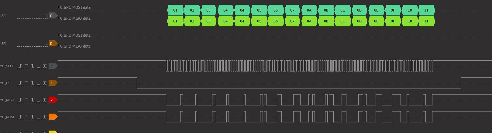
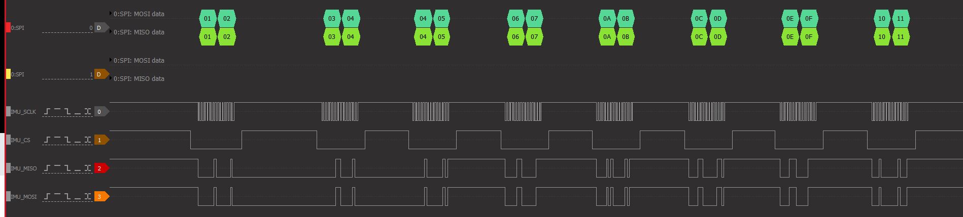
IMU_BURST When the IMU_BURST bit is set, each buffered data capture from the IMU is performed as a single SPI burst transaction (drop CS, clock out all data, raise CS). The length of the burst transaction is determined by BUF_LEN. When the IMU_BURST bit is cleared, IMU data is captured using a sequence of 16 bit SPI words. When the selected page is changed to an IMU page (page != (253, 254, 255)), the IMU SPI port will be restored to register mode, regardless of the BUF_CONFIG setting. The IMU burst data capture will be enabled again when page 255 (buffed data capture page) is re-selected, and the IMU_BURST bit is set.
IMU burst data capture (BUF_CONFIG[1] == 1), with IMU SPI MISO wired to MOSI:
Same IMU Data Capture in register mode (BUF_CONFIG[1] == 0):
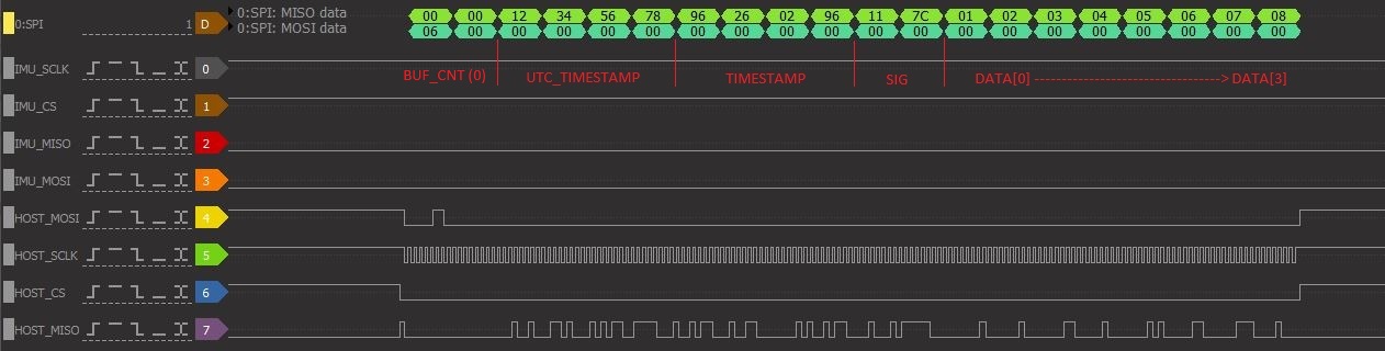
BUF_BURST When the BUF_BURST bit is set and the buffer retrieve register is read, the user SPI interface is configured to clock out the full buffer entry, starting with the timestamp. Multiple buffer burst reads can be chained together by sending a BUF_RETRIEVE read request at the start of the burst data capture, which will trigger a second buffer burst output after the first read is completed, and so on. After a buffer burst output has been enabled, the iSensor-SPI-Buffer slave SPI port will not return to "normal" mode until the full buffer entry has been read (BUF_LEN + 12 bytes clocked out). More detail about the buffer burst output is included in the buffer burst output section
Page: 0xFD (253), Address: 0x04 (4)
| Name | Bits | Description |
|---|---|---|
| 15:0 | LEN | Length (in bytes) of each buffer entry. Valid range 2 - 64. Must be a multiple of 2 (16 bit word size) |
If the IMU_BURST bit of the BUF_CONFIG register is set, the IMU burst word length will be determined by the contents of this register.
Page: 0xFD (253), Address: 0x06 (6)
| Bit | Name | Description |
|---|---|---|
| 15:0 | CMD_MASK | When the user button is pressed, the USER_COMMAND commands corresponding to the bits set in this register are executed. The bits are executed in priority order from LSB to MSB. |
For example, setting this register to 0x800C will trigger a factory reset (0x4), followed by a flash update (0x8) and lastly a software reset (0x8000) when the user button is pressed.
The primary use case for the button is reset and script management (start/stop)
Page: 0xFD (253), Address: 0x08 (8)
| Bit | Name | Description |
|---|---|---|
| 3:0 | DR_SELECT | Select which IMU DIO output pin is treated as data ready. Can only select one pin |
| 4 | DR_POLARITY | Data ready trigger polarity. 1 triggers on rising edge, 0 triggers on falling edge |
| 6:5 | RESERVED | Currently unused |
| 7 | PPS_POLARITY | PPS trigger polarity. 1 triggers on rising edge, 0 triggers on falling edge |
| 11:8 | PPS_SELECT | Select which host processor DIO output pin acts as a Pulse Per Second (PPS) input, for time base synchronization |
| 13:12 | PPS_FREQ | Select the PPS input frequency (10 ^ (PPS_FREQ) Hz). A value of 0 corresponds to a real PPS signal (one pulse per second), which is the recommended mode to use the PPS input. A value of 1 -> 10Hz, 2 -> 100Hz and 3 -> 1000Hz for the PPS input signal. The UTC_TIMESTAMP will be scaled based on the frequency value provided here, to ensure it increments once per second |
| 15:14 | RESERVED | Currently unused |
For each field in DIO_INPUT_CONFIG, the following pin mapping is made:
The following default values will be used for DIO_INPUT_CONFIG:
Page: 0xFD (253), Address: 0x0A (10)
| Bit | Name | Description |
|---|---|---|
| 3:0 | PIN_PASS | Select which pins are directly connected from the host processor to the IMU using an ADG1611 analog switch |
| 7:4 | WATERMARK_INT | Select which pins are driven with the buffer watermark interrupt signal from the iSensor-SPI-Buffer firmware |
| 11:8 | OVERFLOW_INT | Select which pins are driven with the buffer overflow interrupt signal from the iSensor-SPI-Buffer firmware |
| 15:12 | ERROR_INT | Select which pins are driven with the error interrupt signal from the iSensor-SPI-Buffer firmware |
For each field in DIO_OUTPUT_CONFIG, the following pin mapping is made:
The following default values will be used for DIO_OUTPUT_CONFIG:
Page: 0xFD (253), Address: 0x0C (12)
| Name | Bits | Description |
|---|---|---|
| 14:0 | LEVEL | Number of elements stored in buffer before asserting the iSensor-SPI-Buffer data ready interrupt. Range 0 - BUF_MAX_CNT |
| 15 | TOGGLE | When set, the watermark interrupt output will act as a ~10KHz, 50% duty cycle clock output when the watermark interrupt is triggered. If this bit is cleared, the watermark interrupt output is simply pulled high when triggered. |
The watermark interrupt signal is unique in that it can be configured to act as a static active high interrupt signal, or as a "clock" interrupt signal. The clock mode can be useful for devices which trigger reads from an edge.
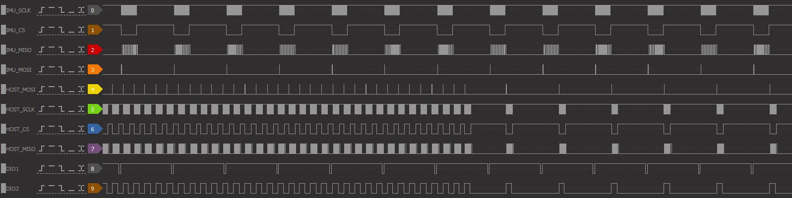
The following capture shows the interrupt behavior with WATERMARK_INT_CONFIG set to 0x8001 (TOGGLE enabled, 1 sample threshold). The attached EVAL-ADIS-FX3 master board is configured to trigger a buffer burst read on the rising edge of DIO2. The iSensor-SPI-Buffer board keeps giving the FX3 master clocks until the buffer is empty, then goes low. Once a new sample has been enqueued from the IMU, another pulse is generated, and clears when the master retrieves the sample.
Page: 0xFD (253), Address: 0x0E (14)
| Name | Bits | Description |
|---|---|---|
| 15:0 | STATUS_MASK | Bitmask to set which bits in the iSensor-SPI-Buffer status register error bits will generate an interrupt when set. Set to 0xFFFF to enable all error interrupts, 0x0000 to disable all. This mask also applies to the error LED on the iSensor-SPI-Buffer, allowing for error detection without reading STATUS. |
Page: 0xFD (253), Address: 0x10 (16)
| Bit | Name | Description |
|---|---|---|
| 7:0 | STALL | Stall time between SPI words (in microseconds). Valid range 2us - 255us |
| 8 | SCLK_SCALE_2 | Sets SCLK prescaler to 2 (18MHz) |
| 9 | SCLK_SCALE_4 | Sets SCLK prescaler to 4 (9MHz) |
| 10 | SCLK_SCALE_8 | Sets SCLK prescaler to 8 (4.5MHz) |
| 11 | SCLK_SCALE_16 | Sets SCLK prescaler to 16 (2.25MHz) |
| 12 | SCLK_SCALE_32 | Sets SCLK prescaler to 32 (1.125MHz) |
| 13 | SCLK_SCALE_64 | Sets SCLK prescaler to 64 (562.5KHz) |
| 14 | SCLK_SCALE_128 | Sets SCLK prescaler to 128 (281.25KHz) |
| 15 | SCLK_SCALE_256 | Sets SCLK prescaler to 256 (140.625KHz) |
The default IMU_SPI_CONFIG value provides an SCLK of 1.125MHz with a stall of 15us. This configuration limits SPI throughput, but should work with all iSensor IMU products. The SPI settings should generally be adjusted to ensure best throughput based on the device in use.
Page: 0xFD (253), Address: 0x12 (18)
| Bit | Name | Description |
|---|---|---|
| 0 | CPHA | SPI clock phase |
| 1 | CPOL | SPI clock polarity |
| 2 | MSB_FIRST | 1 = transmit MSB first, 0 = transmit LSB first |
| 7:3 | RESERVED | Currently unused |
| 15:8 | KEY | The KEY field must be set to 0xA5 for a write to USER_SPI_CONFIG to be processed. Any other value will result in the write being rejected, and no change made to the user SPI port functionality. This prevents inadvertent changing of the SPI mode |
Page: 0xFD (253), Address: 0x14 (20)
| Bit | Name | Description |
|---|---|---|
| 0 | USB_STREAM | USB data stream running (stream command received). If SD_STREAM is set this bit will be cleared (USB streams have lower priority). This bit is volatile (cannot be set in flash). |
| 1 | SD_STREAM | SD card data stream running (stream command executed as part of SD script execution process). SD card data streams have priority over a USB CLI stream. This bit is volatile (cannot be set in flash). |
| 2 | USB_ECHO_DISABLE | Disable command echo to USB CLI. By default, all characters sent to the CLI input are echoed to the output. Disabling this functionality allows for easier CLI scripting from a host device (don't have to discard command echo back after transmitting a command). |
| 3 | SCRIPT_AUTORUN | Start executing an SD card script automatically after the iSensor-SPI-Buffer firmware has finished initialization. This is equivalent to sending a SCRIPT START command immediately after the initialization process has finished |
| 7:4 | RESERVED | Currently unused |
| 15:8 | DELIM | Register read value delimiter character, in ASCII, for the CLI. Defaults to space character |
For more details on the iSensor-SPI-Buffer USB CLI, see the USB_CLI document
For more details on the iSensor-SPI-Buffer SD Card data logging CLI, see the SD Scripts document
Page: 0xFD (253), Address 0x16 (22)
| Bit | Name | Description |
|---|---|---|
| 0 | CLEAR_BUF | Clears any stored buffer contents |
| 1 | CLEAR_FAULT | Clears any fault data logged in flash memory. Until this command is run, status FAULT bit will never clear |
| 2 | FACTORY_RESET | Restores firmware to a factory default state. This command only changes register values in SRAM - to permanently save settings a flash update command must also be issued |
| 3 | FLASH_UPDATE | Save all non-volatile registers to flash memory. The saved values will be persistent through reset events until another flash update command is issued |
| 4 | PPS_ENABLE | Enable PPS timestamp synchronization. Must have PPS_SELECT defined before enabling PPS. The UTC timestamp will start counting up on the next PPS signal |
| 5 | PPS_DISABLE | Disable PPS timestamp synchronization. The microsecond timestamp register will continue free running |
| 6 | SCRIPT_START | Start executing a script from a connected SD card. The script will be loaded from the script.txt file in an attached FAT32 formatted SD card. If any error occurs nothing will be executed, and a script error will be flagged in the STATUS register. In addition, a detailed error will be reported to SCRIPT_ERROR |
| 7 | SCRIPT_CANCEL | Cancel a running script, close any open SD card files, and unmount the SD card file system |
| 8 | WATERMARK_SET | Automatically set the watermark interrupt level for ideal stream operation over the USB command line interface |
| 9 | SYNC_GEN | Start generating sync clock on DIO2_Slave, based on the frequency provided in SYNC_FREQ |
| 12:10 | RESERVED | Currently unused |
| 13 | DFU_REBOOT | Reboot the iSensor-SPI-Buffer into DFU mode. The DFU bootloader stored to ROM will enumerate as an ST USB DFU device which supports firmware updates through the standard ST DFU utility, allowing firmware changes without any external debugger hardware |
| 14 | IMU_RESET | Drive the IMU reset pin low for 1ms, then back high. The user application will have to wait for the reset time of the IMU before reading IMU registers via passthrough. This feature is only implemented on hardware revision C or newer |
| 15 | RESET | Software reset the iSensor-SPI-Buffer firmware |
While commands are being executed, the iSensor-SPI-Buffer slave SPI port is disabled, and all interrupt signals are brought low.
Page: 0xFD (253), Address 0x18 (22)
| Bit | Name | Description |
|---|---|---|
| 15:0 | FREQ | The frequency (in Hz) for the sync signal which can be applied to DIO2_Slave |
Sync generation must be started using the SYNC_GEN command. Sync generation can be stopped by writing to DIO_OUTPUT_CONFIG, which will reset the pin to GPIO mode. The generated sync signal has three primary use cases:
Page: 0xFD (253), Address 0x34 - 0x3A (52 - 58)
| Bit | Name | Description |
|---|---|---|
| 15:0 | SCR | User scratch register. Available for end user use |
Page: 0xFD (253), Address 0x3C (60)
| Bit | Name | Description |
|---|---|---|
| 15:0 | UTC_TIME | Lower 16 bits of the 32-bit UTC timestamp |
Page: 0xFD (253), Address 0x3E (62)
| Bit | Name | Description |
|---|---|---|
| 15:0 | UTC_TIME | Upper 16 bits of the 32-bit UTC timestamp |
The UTC timestamp is a 32-bit value which represents the number of seconds since Jan 01 1970. This register must be set by a master device (no RTC). When a PPS input is enabled using the command register PPS_ENABLE bit, and a PPS pin assigned in DIO_INPUT_CONFIG, this register will count up once per PPS interrupt.
Writing to any byte of the 32-bit UTC timestamp will clear the current 32-bit microsecond timestamp (TIMESTAMP).
Page: 0xFD (253), Address 0x40 (64)
Page: 0xFF (255), Address 0x02 (2)
| Bit | Name | Description |
|---|---|---|
| 0 | BUF_WATERMARK | Set when buffer watermark interrupt condition is met (data ready interrupt) |
| 1 | BUF_FULL | Set when buffer is full (overflow interrupt) |
| 2 | SPI_ERROR | SPI error reported by the user SPI or IMU SPI peripheral |
| 3 | SPI_OVERFLOW | User SPI data overflow (min stall time violated). This bit is set when a user SPI interrupt is received, and the previous user SPI interrupt is still being processed |
| 4 | OVERRUN | Data capture overrun. Set when processor receives an IMU data ready interrupt and has not finished the previous data capture |
| 5 | DMA_ERROR | Set when processor DMA peripheral reports an error (user SPI DMA for burst read or IMU SPI DMA) |
| 6 | PPS_UNLOCK | Set when the PPS synchronization clock is enabled, but no PPS signal has been received for over 1100ms. This flag will also set if the measured period of the provided PPS input has an error of greater than 1% |
| 7 | TEMP_WARNING | Set when the SPI buffer internal temperature sensor (value output to TEMP register) measures a value outside the safe operating range [-40C - 85C] |
| 9:8 | RESERVED | Currently unused |
| 10 | SCRIPT_ERROR | Set when there is an error launching a script from an attached SD card. This bit can be set in one of three ways: If there is no attached SD card, if the attached SD card is not formatted correctly or does not contain script.txt, or if script.txt contains invalid script entries. |
| 11 | SCRIPT_ACTIVE | Set by firmware while an SD card script is being executed. A running script must either terminate by itself, or be cancelled via a SCRIPT_CANCEL command. Resetting the iSensor-SPI-Buffer while a script is executing may cause data corruption on the SD card. This bit is sticky (does not clear on read) and clears automatically when the script execution process ends. This allows for monitoring of the script execution process via the error interrupt output and error LED |
| 12 | FLASH_ERROR | Set when the register signature stored in flash (stored during flash update) does not match signature calculated from SRAM register contents at initialization. Sticky |
| 13 | FLASH_UPDATE_ERROR | Set when the flash update routine fails. Sticky |
| 14 | FAULT | Set when the processor core generates a fault exception (bus fault, memory fault, hard fault, initialization error). Fault exceptions will force a system reset. Sticky |
| 15 | WATCHDOG | Set when the processor has reset due to a watchdog timeout (2s period). Sticky |
Excluding bits identified as sticky, this register clears on read. The values in this register are used to generate an error interrupt, if error interrupts are enabled.
Page: 0xFD (253), Address 0x42 (66)
| Bit | Name | Description |
|---|---|---|
| 4:0 | FAULT_SRC | Fault source value. Fault types are defined in flash module https://ajn96.github.io/iSensor-SPI-Buffer/flash_8h.html |
| 15:5 | RESERVED | Currently unused |
The FAULT_CODE register is stored on a different flash page from the register array. It can only be cleared with a CLEAR_FAULT command.
Page: 0xFD (253), Address 0x44 (68)
Page: 0xFF (255), Address 0x04 (4)
| Bit | Name | Description |
|---|---|---|
| 15:0 | CNT | Number of entries currently stored in the buffer. Write 0 to clear buffer while on page 255. All other writes ignored |
Page: 0xFD (253), Address 0x44 (70)
| Name | Bits | Description |
|---|---|---|
| 15:0 | MAX | Total number of entries which can be stored in the buffer. Updates automatically when BUF_LEN is changed |
Page: 0xFD (253), Address 0x4A (74)
| Bit | Name | Description |
|---|---|---|
| 15:0 | TIMESTAMP | Lower 16 bits of the 32-bit microsecond timestamp |
Page: 0xFD (253), Address 0x4C (76)
| Bit | Name | Description |
|---|---|---|
| 15:0 | TIMESTAMP | Upper 16 bits of the 32-bit microsecond timestamp |
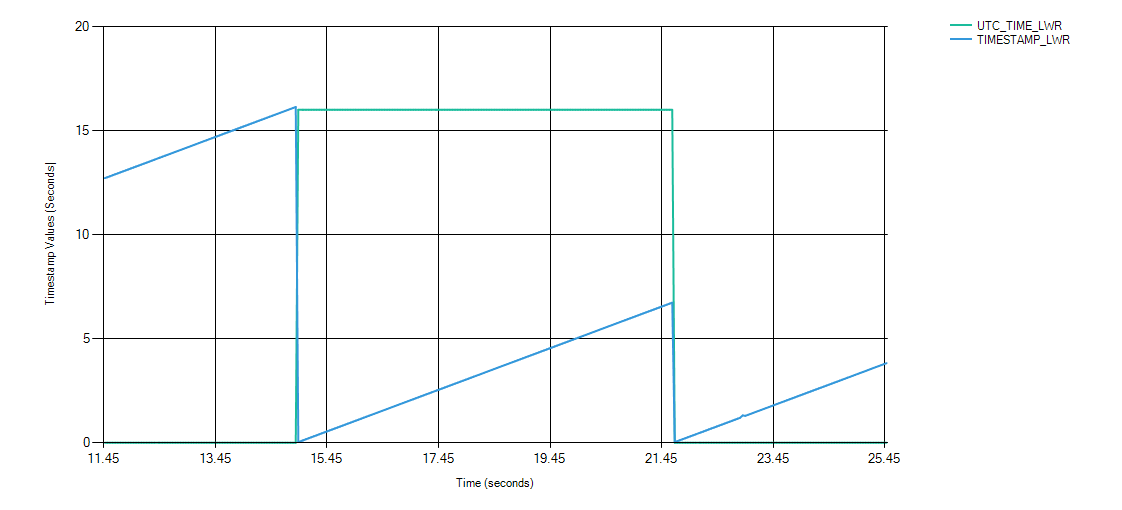
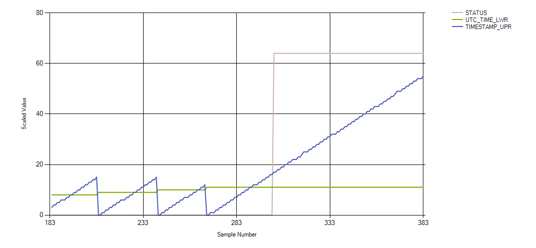
These combined registers form a 32-bit microsecond timestamp which starts counting up as soon as the iSensor-SPI-Buffer firmware finishes initialization and enters its cyclic executive loop.
When a pulse per second (PPS) input is enabled using the PPS_ENABLE command, and a PPS pin is assigned in DIO_INPUT_CONFIG, this microsecond timestamp will reset to 0 every time a PPS pulse is received. This PPS functionality allows the iSensor-SPI-Buffer firmware to track the "wall" time with microsecond accuracy and high long term stability (from PPS clock). Since the microsecond timestamp is reset every second, any error accumulation (due to 20ppm crystal) should be minimal.
The plot below shows the UTC_TIME_LWR and TIMESTAMP_UPR register with a 1Hz PPS signal applied. Each time a PPS edge is received, the TIMESTAMP_UPR (and lower, not shown) are reset to 0, and the UTC_TIME_LWR register increments.

If the PPS signal is lost, the internal microsecond timer will continue counting up, and the STATUS PPS Unlock bit will set. This allows a master device to continue tracking sample timestamps for a significant time even if the PPS signal is lost. The plot below shows that behavior.
Page: 0xFD (253), Address 0x4E (78)
| Bit | Name | Description |
|---|---|---|
| 15:0 | TEMP | Temp sensor output. 1 degree C = 10LSB. Value of 0LSB -> 0C |
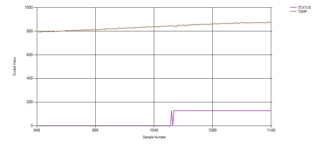
This value is sourced from the thermistor embedded in the STM32F303 package. The temperature value is scaled using a two point temperature calibration provided by ST (measurements taken at 30C and 110C). Even though temperature output is calibrated, the measurement is very susceptible to heat from the STM32 processor core. If the temperature measurement ever goes out of range [-40C to 85C] a temperature warning flag will be set in the STATUS register.
The measured value of VDD is used to normalize the TEMP_OUT register value to a 3.3V ADC reference voltage. This normalization ensures good temperature sensor linearity across the valid supply range for the device (TEMP will no longer shift with voltage, as shown here). The downside of normalizing the measured temperature value with the measured Vdd value is that the noise of the temp sensor measurement increases, but this is an acceptable tradeoff.
Page: 0xFD (253), Address 0x50 (80)
| Bit | Name | Description |
|---|---|---|
| 15:0 | VDD | Measured Vdd output. 1V = 100LSBs (3.3V -> 330) |
The value of Vdd is calculated by measuring the value of VREFINT (internal regulated voltage reference) using the ADC and comparing against the expected measurement, with Vdd = 3.3V. Changes in Vdd (VREF) will cause an apparent change in the VREFINT measurement, which can be used to calculate Vdd.
Page: 0xFD (253), Address 0x64 (100)
| Bit | Name | Description |
|---|---|---|
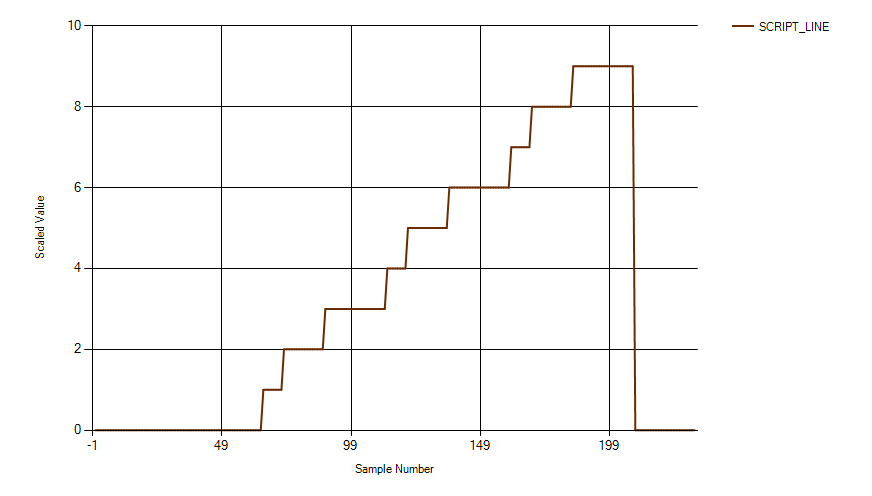
| 15:0 | LINE | Line number in the provided SD card script (script.txt) which is currently being executed by the script execution engine. Will be set to zero when there is no script running. |
The image below shows the script line number value as a simple script executes:
sleep 1f4
sleep 3e8
sleep 5dc
sleep 1f4
sleep 3e8
sleep 5dc
sleep 1f4
sleep 3e8
sleep 5dc
Page: 0xFD (253), Address 0x66 (102)
| Bit | Name | Description |
|---|---|---|
| 0 | NO_SD | Set when a script start command is processed and there is no SD card attached. This is determined using the SD card detect pin. When this condition is detected, the script start process is aborted. |
| 1 | MOUNT_ERROR | Set when the FAT file system fails to mount the SD card during the script setup process. When this condition is detected, the script start process is aborted. |
| 2 | SCRIPT_OPEN_ERROR | Set when the software cannot open "script.txt" in read only mode during the script setup process. When this condition is detected, the script start process is aborted. |
| 3 | RESULT_OPEN_ERROR | Set when the software cannot open "result.txt" in write mode during the script setup process. When this condition is detected, the script start process is aborted. |
| 4 | PARSE_INVALID_CMD | Set when the software opens script.txt for parsing, but one of the lines contains an invalid command. When this condition is detected, the script start process is aborted. |
| 5 | PARSE_INVALID_ARGS | Set when the software opens script.txt for parsing and detects a valid command with invalid arguments provided. When this condition is detected, the script start process is aborted. |
| 6 | PARSE_INVALID_LOOP | Set when the software opens script.txt for parsing and detects an invalid loop structure. Loops have a fixed loop count, and cannot be nested. When this condition is detected, the script start process is aborted. |
| 7 | WRITE_FAIL | Set when a running script tries to write data to the output file and gets an error. This error does not stop the script execution process. |
| 15:8 | RESERVED | Currently unused |
The script error register is set to 0 when a script start or cancel command is received. Any errors which occur during the script load, parse, and execution process are bit or'd into this register.
Page: 0xFD (253), Address 0x6E (110)
| Bit | Name | Description |
|---|---|---|
| 7:0 | MINOR | Minor firmware revision number, in BCD |
| 14:8 | MAJOR | Major firmware revision number, in BCD (second digit limited to 7, giving max possible firmware rev 79.99) |
| 15 | DEBUG | Set if the running firmware was compiled with debug flags enabled. The recommended way to use the iSensor-SPI-Buffer firmware is in release mode (DEBUG = 0). |
This rev corresponds to the release tag for the firmware. For example, rev 1.15 would be represented by 0x0115 in FW_REV.
Page: 0xFD (253), Address 0x70 (112)
| Bit | Name | Description |
|---|---|---|
| 7:0 | MONTH | Firmware program month, in BCD |
| 15:8 | DAY | Firmware program day, in BCD |
For example, April 24th would be represented by 0x2404. The DAY/MONTH/YEAR values are generated automatically at compile time using the C DATE preprocessor macro.
Page: 0xFD (253), Address 0x72 (114)
| Bit | Name | Description |
|---|---|---|
| 15:0 | YEAR | Firmware program year, in BCD |
For example, the year 2020 would be represented by 0x2020. The DAY/MONTH/YEAR values are generated automatically at compile time using the C DATE preprocessor macro.
Page: 0xFD (253), Address 0x74 - 0x7E (116 - 126)
| Bit | Name | Description |
|---|---|---|
| 15:0 | SN | These six registers contain the 96 bit unique serial number in the STM32 processor core |
Page: 0xFE (254), Address 0x12 - 0x50 (18 - 80)
| Bit | Name | Description |
|---|---|---|
| 15:0 | WRITE_N | Write data to transmit on MOSI line while capturing a buffered data entry |
Page: 0xFE (254), Address 0x7C (124)
| Bit | Name | Description |
|---|---|---|
| 15:0 | CHKSUM | Derived signature for all registers stored to flash memory. This value is determined at initialization and compared to "FLASH_SIG" to determine if flash memory contents are valid |
Page: 0xFE (254), Address 0x7E (126)
| Bit | Name | Description |
|---|---|---|
| 15:0 | CHKSUM | Signature for all registers stored to flash memory. This value is stored in flash, and is updated when a flash update command is executed |
Page: 0xFF (255), Address 0x06 (6)
| Bit | Name | Description |
|---|---|---|
| 15:0 | RETRIEVE | Read to place a new sample from the buffer into the BUF_READ output registers. Will always contain 0 |
Page: 0xFF (255), Address 0x08 (8)
| Bit | Name | Description |
|---|---|---|
| 15:0 | TIMESTAMP | Lower 16 bits of the 32-bit buffer entry UTC timestamp value which is stored at the start of each data capture. Resolution: 1LSB = 1 second (driven by PPS input) |
Page: 0xFF (255), Address 0x0A (10)
| Bit | Name | Description |
|---|---|---|
| 15:0 | TIMESTAMP | Upper 16 bits of the 32-bit buffer entry UTC timestamp. |
Page: 0xFF (255), Address 0x0C (12)
| Bit | Name | Description |
|---|---|---|
| 15:0 | TIMESTAMP | Lower 16 bits of a 32-bit buffer entry timestamp value which is stored at the start of each data capture. Resolution: 1LSB = 1us |
Page: 0xFF (255), Address 0x0E (14)
| Bit | Name | Description |
|---|---|---|
| 15:0 | TIMESTAMP | Upper 16 bits of a 32-bit buffer entry timestamp. |
Page: 0xFF (255), Address 0x10 (16)
| Bit | Name | Description |
|---|---|---|
| 15:0 | SIGNATURE | Buffer signature. This is the sum of all 16-bit words stored in the buffer (including timestamp) |
Page: 0xFF (255), Address 0x12 - 0x50 (18 - 80)
| Bit | Name | Description |
|---|---|---|
| 15:0 | READ_N | Read data received on the MISO line while capturing a buffered data entry |
Burst output functionality for buffered data is provided to allow faster dequeuing of accumulated buffer entries over the user SPI port. Each burst buffer output includes all the data from a single buffer entry, and can be read without toggling chip select, allowing for significantly faster throughput. In addition, the data is moved from the buffer output register to the user SPI port using a DMA peripheral, which offloads work from the CPU. This potentially allows for higher IMU data rates, without experiencing overrun.
| SPI Word Number (16 bit words) | Master -> iSensor-SPI-Buffer | iSensor-SPI-Buffer -> Master |
|---|---|---|
| 0 | 0x0600 | BUF_CNT (after dequeue) |
| 1 | 0x0000 (Don't care) | BUF_UTC_TIME_LWR |
| 2 | 0x0000 (Don't care) | BUF_UTC_TIME_UPR |
| 3 | 0x0000 (Don't care) | BUF_TIMESTAMP_LWR |
| 4 | 0x0000 (Don't care) | BUF_TIMESTAMP_UPR |
| 5 | 0x0000 (Don't care) | BUF_SIG |
| 6 | 0x0000 (Don't care) | BUF_DATA_0 |
| n | 0x0000 (Don't care) | BUF_DATA_N |
The image below shows the buffer burst output format with BUF_LEN set to 8 bytes, and the IMU MOSI wired to IMU MISO (BUF_WRITE[n] -> BUF_DATA[n]). The UTC timestamp was set to 0x56781234.